
On to the second Memory Boy. I was hoping this would be the same problem again, but this one fought me.

After opening it, it was apparent that someone else had been in here before. The ribbon cable to the footswitch had been replaced with discrete wires and there was a large splash of solder hanging off an electrolytic cap on the main board. I have no idea if the ribbon actually failed or if the last person to work on this was just trying things, they tend to be reliable.
This one also had no wet signal. Power was OK, I checked the CLK testpoint and it also had no clock waveform. I replaced the 4011 hoping I was done, but still nothing. At this point I thought about replacing the LM13700 as well, but decided to trace out the daughterboard to see what it was actually doing. I remembered to take pictures of both sides of the PCBs this time.
 |
| Main PCB, backside |
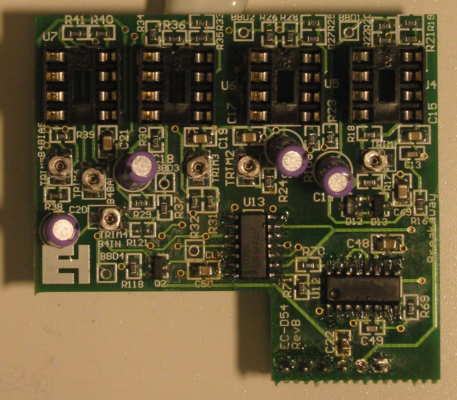 |
| BBD board |
 |
| BBD board, backside |
It's not unusual when doing this that the problems reveals itself halfway through tracing out the circuit. In this case I found that I had no continuity between pin 2 of the header that connects the boards and pin 1 of the LM13700 (bias input), despite a track on the PCB clearly running between the two. I can only guess that the daughterboard was rocked on the header strip and this trace cracked. I ran a jumper wire between the header and the OTA and I had a clock signal again. Still no wet sound, which was worrying as it suggested the BBDs were bad. Fortunately, it seemed that the last repairperson also played with the bias trimpots, and after re-biasing each stage I had a working delay. Unfortunately, no schematics for everyone else, at least not yet.
 |
| Jumper wire from U12 to connector pin 2 |
This one sounds identical to the other, so unless I decide to try out some modifications I'll sell one (or both).
No comments:
Post a Comment