Thursday 31 January 2019

Another Electro-Harmonix Freeze

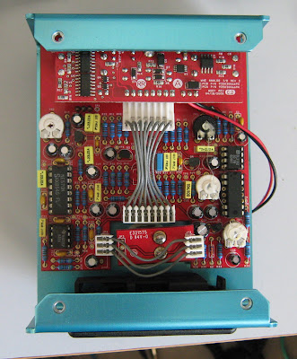
I got another Electro-Harmonix Freeze fairly cheap, it sounded like it had been killed by an incorrect wrong power supply. I took it apart and found that it was a newer revision than I had seen before, the board was EC-D68 Rev C (the last one was Rev B). The main difference I notice was an AK4558 codec instead of PCM3052A.

Freeze Rev C PCB, flash ROM temporarily removed.
Main PCB, LM317 temporarily removed.

There was no sign of life, I found that the series Schottky diode at the 9V input had failed open-circuit and that the LM317 had an internal short between it's input and output pins. The fast/slow/latch mode switch also fell to pieces when the board came out of the enclosure.

I replaced the bad diode with an SS14L (it was the correct size and I already had some at hand) and installed a new LM317. I thought that the LM317 was supplying 3.3V to the DSP and this would fix everything. Instead, the pedal would pass a clean signal but with a clicking sound once or twice per second. I found out that LM317 is actually used as a 1.25V regulator, which is only used for the analog VCC of the DSP56374.

I thought the clicking may be the DSP watchdog timer firing, possibly because it was missing program code, so I removed the flash memory and dumped it. It was a perfect match for the dump I made of the first pedal I repaired, so no problem there.

Measuring power at every IC I found that the 5V rail was high at around 5.9V and the 3.3V supply was sitting at 3.9V. I thought that U5 and U8 (both SOT-89 packages) were also voltage regulators and that maybe they had been damaged as well. I also noticed that U6 is connected to the reset pin of the DSP, and it was resetting the DSP every second or so. My guess is that U6 (also connected to the 3.3V supply) is some kind of voltage supervisor and it is resetting the DSP because of an incorrect 3.9V at VCC.

I found a great picture at freestompboxes (thanks to Steven_M!) showing that on previous version, U5 was 78L05 (5V regulator) and U8 was BA932 (who knows, but from context it has to be a 3.3V regulator).

U5 & U8 on another revision.

The Rev C board in front of me had "BA420" on both chips. Possibly EHX decided to run all 5V parts off of 3.3V, and doubled up on regulators? I don't know.an

To test this out, I decided to remove both chips and apply 5V and 3.3V from  external power supplies.

U5 & U8 removed, external power applied

This set up was a little awkward, but everything work correctly. Current draw looked totally reasonable, 19mA from the 5V supply and 21mA from the 3.3V. No resetting, no clicking, and the pedal could freeze audio in all 3 modes.

Current draw on 5V and 3.3V supplies.

I ordered L78L05ABUTR and MCP1804T-3302I/MB as replacement 5V and 3.3V SOT-89 regulators. I also used 2MD3T2B2M2RE as a replacement switch. This replacement is not threaded for a nut, but recent version of the Freeze don't look like they are threaded either. Pedal works like new.


Ibanez DDL10 Delay II

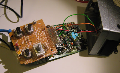
This is another early digital delay pedal, I am guessing it was built in 1986 from some of the IC date codes. I don't know if the 10 series included the first Ibanez/Maxon digital delay. Obviously this is the "Delay II", but the DDL Delay I and Delay III were also released in the same series of pedals,  each with different delay times. The max delay time of 900ms of the Delay II put it in a similar league to the Boss DD-2.


Inside, there is a two PCB construction with a hard-wired ribbon cable. The top board has unpopulated parts, I would guess that a DML10 (modulated delay) could be built on this same board by populating an opamp LFO and adding the two extra pots.

DDL10 internals

The bottom PCB has two 4164 DRAMs, an NE571 compoundor, LM311 comparator (most likely used as part of an ADC as in the DD-2 and PDS delays) and a bunch of opamps. The SIL (single in-line) package chips are M5218L low-noise preamplifiers, used in lots of Japanese pedals. There are only 2 4164 64kb DRAMs, the DD-2 has 3. Either the DD-3 has higher sampling rates, or the Ibanez uses 8-bit samples instead of 12-bit. This is still more than the single 64k seen in Digitech PDS 1 second delays.

Main PCB, component side

The back side of the lower board just has a main controller MC4101F IC. I can't find any info on this, it's almost certainly a custom controller for digital delays (like the Boss/Roland RDD63H101).

Main PCB, back-side.

This unit looked mostly dead, it passed no effected signal and LED didn't respond to the footswitch. I thought the back of the larger board looked a bit crusty so I clean it with 99% IPA, afterwards I saw the LED blink with the footswitch. Still no signal.

I couldn't find any schematics for this model online, but someone has scanned and uploaded an Ibanez factory schematic for the DFL10 flanger from the same series, which uses the same controller IC. There is a full pinout.

DFL10 schematic page 1.
DFL10 schematic page 2.

From the schematic, the clock signal for the controller looked like it was coming from a VCO to pin 26 ("2F"). I probed my board and found that I did have a clock signal, it could be varied by turning the Delay knob, and I also had what looked like communication between the controller and the RAM chips.

At this point I got really lucky. There was a 100uF electrolytic capacitor near the LM311 comparator that was a little discoloured. While taking measurements I noticed it was getting warm. I pulled it from the circuit, and the pedal started passing a delayed signal. This cap is connected from 5V to ground right next to the comparator input, if the cap was leaky then it would effectively mute the comparator. Everything worked without this capacitor, I replaced it anyway with a new low profile 100uF for peace of mind.

Faulty capacitor pulled.
The LED turned out to be a bad solder joint - it would light sometimes if it was held in a certain position. Reflowing the joints fixed it.

Way Huge Aqua Puss MK II

I don't think I've ever looked at anything by Way Huge before. This is a modern version of the Aqua-Puss, and Jim Dunlop acquired Way Huge in 2006, so I expect it to be similar to the current Dunlop and MXR stuff.

This one would light it's LED when switched on but wouldn't pass a signal.


The insides are really nice, and very easy to disassemble. There are three PCBs - one just breaking out the switch contacts, one SMD board for input/output and switching and one through-hole board with the effect guts. They probably re-use the two smaller PCBs for all of the pedals in this size of enclosure.

Interior

The upper board has a CD4013 dual flip-flop, a CD4093B quad NAND gate and a relay to handle the bypass. The manual says the pedal has "AC protection", I don't know if this is just a series Shottky diode or something more sophisticated. There are some opamps and what looks like a IRF7606 Mosfet in a micro-8 package, that could be doing some power switching in case of reverse polarity or an AC supply connected. Relay is a EA2-5SNJ, similar to what's in a DL4.

I/O & switching board component side

Jack side

The delay board a V3205 BBD and BL3102 clock generator, SA571 compoundor and LF353 opamp for input and output buffering. Freestompboxes.org has the full schematic, it's not too complex a delay and similar to a DM-2/DM-3.

Pinout of the 8-pin connector is as follows (taking the pin with square PCB footprint as pin 1)
  1. 9V
  2. Ground
  3. LED
  4. Bypass switch
  5. Input signal
  6. Output signal
  7. Relay coil
  8. Relay coil 
The relay coil contacts are probably only broken out so the small PCB can be connected to a test jig, the main board doesn't route them anywhere.

Delay board component side

Delay board back side


I couldn't tell if the relay was actually switching, as it was hard to hear it click over the sound of the footswitch. When I disconnected the foot switch board and triggered the switch with some wire I could hear the relay clicking, so the switching logic was probably good.

After hooking up a test signal and oscilloscope I could see that the input signal was reaching the first opamp stage but there was nothing at the output pin. I desoldered the LF353 and replaced it with a socket and a TL072 for now.

Removed LF353

Now I had a clean signal in bypassed mode, but no delay. No switching waveforms on the BBD on the oscilloscope. No power at either the clock generator or BBD either. The schematic shows an NPN transistor/diode voltage regulator for these chips, I found that the 2N3904 transistor was blown to shit! After replacing with a new 2N3904 it regulator to around 7.4 volts. I'm not totally sure why this is needed as the BL3102 & V3205 should be happy to run on 9V, this may be a holdover from using older BBD chips. (Update: it turns out that there are multiple V3205 datasheets online, with conflicting information. According to Coolaudio, the max Vdd for a V3205SD is 8V).

Epoxy case blown off voltage regulator pass transistor. I don't know how I missed this.

I could now see clock signal at the BBD which varied with the delay knob as expected, but still no delay. I could see an input signal at pin 11 of the SA571 but nothing at the output on pin 10. I borrowed an SA570 from PDS delay pedal and this brought back the delay effect. Sounds great but not too different from other analog delays I have.

So: dead 2N3904 regulator, dead LF353 and dead SA571. I'm guessing this was fed too high a voltage from the wrong power supply. It's running happily 24 hours later with a new SA571 so this will probably go up for sale on Reverb pretty soon.