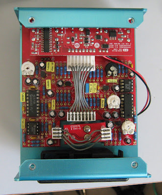
I don't think I've ever looked at anything by Way Huge before. This is a modern version of the Aqua-Puss, and Jim Dunlop acquired Way Huge in 2006, so I expect it to be similar to the current Dunlop and MXR stuff.
This one would light it's LED when switched on but wouldn't pass a signal.

The insides are really nice, and very easy to disassemble. There are three PCBs - one just breaking out the switch contacts, one SMD board for input/output and switching and one through-hole board with the effect guts. They probably re-use the two smaller PCBs for all of the pedals in this size of enclosure.
 |
| Interior |
The upper board has a CD4013 dual flip-flop, a CD4093B quad NAND gate and a relay to handle the bypass. The manual says the pedal has "AC protection", I don't know if this is just a series Shottky diode or something more sophisticated. There are some opamps and what looks like a IRF7606 Mosfet in a micro-8 package, that could be doing some power switching in case of reverse polarity or an AC supply connected. Relay is a EA2-5SNJ, similar to what's in a DL4.
 |
| I/O & switching board component side |
 |
| Jack side |
The delay board a V3205 BBD and BL3102 clock generator, SA571 compoundor and LF353 opamp for input and output buffering. Freestompboxes.org has the full schematic, it's not too complex a delay and similar to a DM-2/DM-3.
Pinout of the 8-pin connector is as follows (taking the pin with square PCB footprint as pin 1)
- 9V
- Ground
- LED
- Bypass switch
- Input signal
- Output signal
- Relay coil
- Relay coil
 |
| Delay board component side |
 | |||||||||||||||||||||||||
| Delay board back side |
I couldn't tell if the relay was actually switching, as it was hard to hear it click over the sound of the footswitch. When I disconnected the foot switch board and triggered the switch with some wire I could hear the relay clicking, so the switching logic was probably good.
After hooking up a test signal and oscilloscope I could see that the input signal was reaching the first opamp stage but there was nothing at the output pin. I desoldered the LF353 and replaced it with a socket and a TL072 for now.
 |
| Removed LF353 |
Now I had a clean signal in bypassed mode, but no delay. No switching waveforms on the BBD on the oscilloscope. No power at either the clock generator or BBD either. The schematic shows an NPN transistor/diode voltage regulator for these chips, I found that the 2N3904 transistor was blown to shit! After replacing with a new 2N3904 it regulator to around 7.4 volts. I'm not totally sure why this is needed as the BL3102 & V3205 should be happy to run on 9V, this may be a holdover from using older BBD chips. (Update: it turns out that there are multiple V3205 datasheets online, with conflicting information. According to Coolaudio, the max Vdd for a V3205SD is 8V).
 |
| Epoxy case blown off voltage regulator pass transistor. I don't know how I missed this. |
I could now see clock signal at the BBD which varied with the delay knob as expected, but still no delay. I could see an input signal at pin 11 of the SA571 but nothing at the output on pin 10. I borrowed an SA570 from PDS delay pedal and this brought back the delay effect. Sounds great but not too different from other analog delays I have.
So: dead 2N3904 regulator, dead LF353 and dead SA571. I'm guessing this was fed too high a voltage from the wrong power supply. It's running happily 24 hours later with a new SA571 so this will probably go up for sale on Reverb pretty soon.
Hello from France,
ReplyDeleteRealy good job You made.
I was looking to mute the dry signal to only have a 100% wet effect. When the pedal is ON, Do You have any idea where I can intercept the dry signal and mute it (with toggle switch) ?
Or have You a better way to do this ?
Best regards,
Ju'
Looks like C2 is vented as well, which is further evidence of over (or reverse) voltage which caused the damage.
ReplyDelete