Showing posts with label Analog delay. Show all posts

Thursday, 14 February 2019

Another Ibanez ES2 Echo Shifter repair

I took another look at an Ibanez Echo Shifter that I had previously repaired, but had come back to me. This time it wouldn't light up, but did pass a clean signal. I suspected a bad power supply for the digital section.

I opened it up, and I could see ~8.5V volts powering the opamps but no voltage at any of the digital parts, where I would expect 3.3V.

Way back in July 2017 a commenter asked if I knew what the part number for U14 was, likely to be a buck-converter, and that they suspected it was a Texas Instruments TPS62056. The package, function and chips marking all looked like a perfect match so I ordered a few this week to see if it was right.

Before

Desoldering was straight-forward, I used hot air and kapton for protecting parts I didn't want to overheat.

During

The new chip has near identical markings to the old one. Re-soldering was a little harder as there isn't a lot of space, I ended up removing C73 temporarily to get better access. The bridged pins are fine, all those pins are connected together at the PCB.

After

Everything works again with the new chip. Thanks to Shane Bussiere for doing the research and sharing the part number, sorry I didn't help out.

All working again.

Looking at the TPS62056 datasheet, I can guess why this failed. The buck converter chip has a maximum Vin of 10V, the Echo Shifter runs the power jack through a series Schottky diode for polarity protection and then to the TPS. If you use a 9V power supply the chip gets around 8.6V, which is fine, but using a 12V power supply or higher will probably kill it. I couldn't find a compatible chip from TI with the same footprint and pinout but higher maximum input voltage, let me know if one exists.

I would really like to modify this to add a modulation rate control. I hunted around for modulation signals and unfortunately there doesn't seem to be a LFO onboard, it looks like the modulation is done in software in the ADAU1701 DSP. A modulated square wave is run out of the first audio DAC on pin 46.

While I had this open I desoldered the 24AA128 serial EEPROM and dumped the contents, it can be downloaded here. Afaik the ADAU1701 instruction set is not publicly documented, so I don't think the firmware can be easily modified.

Friday, 8 February 2019

Electro-Harmonix Stereo Memory Man (EH-7811)

The classic, basic, no-frills BBD delay. This is an EH-7811 revision, dating from around 1980 based on IC codes. This version is main powered (240V), runs at +/-15V internally, Panasonic MN3005. There is no LED, I think this was the last version without one. There is an Echo/Chorus switch which probably reduces delay times, and in-phase and out-of-phase outputs for a "stereo" effect.

This is another one that I have had a for a while, and later came back to. I bought this a couple of years ago and nearly got it working, then hit a dead-end.

It was pretty dirty on first inspection, and missing a knob for the blend control. The power cable had been shortened to a ridiculous length, about six inches, making it awkward to work on.

Before cleaning...

The original eBay picture shows this off:


The insides show that the PCB is complete with no obvious damage. It does anchor everything off of board-mounted pots which are only on one side of the large PCB - the other end floats and tends to cantilever.

PCB as received

The delay/chorus switch is almost entirely missing, just the frame left.

Interior of case, Echo/Chorus switch.

Closer inspection of the PCB found that the Blend potentiometer's pads had all craclked off. The pot was still hanging onto the board, but nothing was electrically connected. I ran some small jumpers from the pot back to the nearby traces. I also installed a new sliding switch. I referenced a schematic for the later EH-7811B at David Morrin's excellent site. The main difference (apart from the LED) seems to be that this version has an extra 741 opamp to invert the delay signal for the out-of-phase output.

At this point, I had some signal coming thorough, but hugely distorted. All output opamps were saturated, sitting at ~ 13 or -13 volts. I socketed and replaced some of the opamps with no change. There was a DC offset being introduced somewhere.

I had a few ideas:
  1. dead opamp, or opamp feedback network. No changes when swapping opamps and measuring feedback resistors.
  2. leaking AC-coupling capacitors. I replaced some 1uF caps of a type I had seen fail before with modern film caps, no changes
  3. Missing ground node somewhere...
This went back into the "fix later" box for a while. I dug it out and went over some of schematics for other revisions and noticed that one side of the blend knob should be connected to ground. My blend knob had been cracked off the board, I could barely see a small track below the pot's pads that should have been connecting to ground.

I ran another jumper wire to ground, and now all the outputs were sitting at 0V.


I fitted a new mains cable so that is actually usable. There is no internal fuse, so I changed the cable fuse to a 3A part. I tried the original opamps in the sockets, but the outputs got noticeably more noisy. Maybe semiconductor processing has improved to the point where new 4558s and 741s are less hiss-y.

There was some serious clock whine, especially at long delay times. Fortunately I was able to completely trim this out.

PCB after repairs.

PCB after repairs, parts replacement.

I've said before I haven't noticed huge differences between analog delays based on BBD types. I had the Aqua Puss at hand for comparison between a V3205 and MN3005. The Memory Man sounds cleaner, if that makes sense? Less distortion on each repeat, a bit closer to the original signal. Still sounds like analog delay, just not as overblown.

Reassembled.

Thursday, 31 January 2019

Way Huge Aqua Puss MK II

I don't think I've ever looked at anything by Way Huge before. This is a modern version of the Aqua-Puss, and Jim Dunlop acquired Way Huge in 2006, so I expect it to be similar to the current Dunlop and MXR stuff.

This one would light it's LED when switched on but wouldn't pass a signal.


The insides are really nice, and very easy to disassemble. There are three PCBs - one just breaking out the switch contacts, one SMD board for input/output and switching and one through-hole board with the effect guts. They probably re-use the two smaller PCBs for all of the pedals in this size of enclosure.

Interior

The upper board has a CD4013 dual flip-flop, a CD4093B quad NAND gate and a relay to handle the bypass. The manual says the pedal has "AC protection", I don't know if this is just a series Shottky diode or something more sophisticated. There are some opamps and what looks like a IRF7606 Mosfet in a micro-8 package, that could be doing some power switching in case of reverse polarity or an AC supply connected. Relay is a EA2-5SNJ, similar to what's in a DL4.

I/O & switching board component side

Jack side

The delay board a V3205 BBD and BL3102 clock generator, SA571 compoundor and LF353 opamp for input and output buffering. Freestompboxes.org has the full schematic, it's not too complex a delay and similar to a DM-2/DM-3.

Pinout of the 8-pin connector is as follows (taking the pin with square PCB footprint as pin 1)
  1. 9V
  2. Ground
  3. LED
  4. Bypass switch
  5. Input signal
  6. Output signal
  7. Relay coil
  8. Relay coil 
The relay coil contacts are probably only broken out so the small PCB can be connected to a test jig, the main board doesn't route them anywhere.

Delay board component side

Delay board back side


I couldn't tell if the relay was actually switching, as it was hard to hear it click over the sound of the footswitch. When I disconnected the foot switch board and triggered the switch with some wire I could hear the relay clicking, so the switching logic was probably good.

After hooking up a test signal and oscilloscope I could see that the input signal was reaching the first opamp stage but there was nothing at the output pin. I desoldered the LF353 and replaced it with a socket and a TL072 for now.

Removed LF353

Now I had a clean signal in bypassed mode, but no delay. No switching waveforms on the BBD on the oscilloscope. No power at either the clock generator or BBD either. The schematic shows an NPN transistor/diode voltage regulator for these chips, I found that the 2N3904 transistor was blown to shit! After replacing with a new 2N3904 it regulator to around 7.4 volts. I'm not totally sure why this is needed as the BL3102 & V3205 should be happy to run on 9V, this may be a holdover from using older BBD chips. (Update: it turns out that there are multiple V3205 datasheets online, with conflicting information. According to Coolaudio, the max Vdd for a V3205SD is 8V).

Epoxy case blown off voltage regulator pass transistor. I don't know how I missed this.

I could now see clock signal at the BBD which varied with the delay knob as expected, but still no delay. I could see an input signal at pin 11 of the SA571 but nothing at the output on pin 10. I borrowed an SA570 from PDS delay pedal and this brought back the delay effect. Sounds great but not too different from other analog delays I have.

So: dead 2N3904 regulator, dead LF353 and dead SA571. I'm guessing this was fed too high a voltage from the wrong power supply. It's running happily 24 hours later with a new SA571 so this will probably go up for sale on Reverb pretty soon.

Monday, 1 May 2017

Rozz R8 Repair

Another analog delay with no delayed signal. I had never heard of Rozz (not Ross), apparently it was a brand applied by a Japanese OEM that released pedals under many different names. Effects database found quite a few variants, it seems that the Ampeg rebrand is sought after nowadays.

http://www.effectsdatabase.com/model/guyatone/ps00x/ps006
http://www.effectsdatabase.com/model/westbury/06
http://www.effectsdatabase.com/model/ampeg/a/8
http://www.effectsdatabase.com/model/tora/ts006
http://www.effectsdatabase.com/model/rozz/r/8

Freestompboxes has a schematic for the Guyatone variant. It looks like it was drawn using the official Boss DM-2 schematic as a starting point.

http://freestompboxes.org/viewtopic.php?f=1&t=21461

The narrow English font looks very Japanese.

Inside is a Mitsubishi (Panasonic!) MN3005 BBD and MN3101 clock generator, which is nice. The only other IC is an NE570 compander, all buffering and filtering is done with discrete amplifiers. Otherwise it's similar to the DM-2/AD80 style delays of the time, except that there is no "cancel" trim pot to dial out any clock noise, and the wet and dry signals are passively mixed with no output buffers. This might have been a lower-cost design.

PCB is the usual single-sided type used by Boss in the 80s.


Looking around the board I could see clock signals at the 3101 and BBD, but I was confused as they seemed to disappear when I flipped the board over to see the traces on the solder side. Pushing down on the MN3005 would give a momentary burst of delayed noise, so the delay circuit appeared to work, only with a broken connection somewhere. I moved all the wiring from lap-soldered pads to run through the PCB in case a bad joint was causing the problem. No dice.

Eventually I realised that the trimpot for setting clock rates was broken, it only made contact when the pedal was upside down! After desoldering it literally fell part, the wiper only contacts the conductive track when held in place by gravity.

Original timing trimpot.


With a 100k replacement pot the delayed signal was back. The available delay times were not quite right, it would happily go to ~1/2 second at one end of the pot but the other was not much shorter. Fast short delays were not possible. Clock bleed-through was also really bad, it would whistle at the clock frequency even in bypass mode.


100k temporary replacement.


After finding a 50k replacement things were a lot better. Clock rates were manageable from ~8 kHz up to 15 kz or so, allowing long and short delays. Clock noise dropped a lot but is still audible at long delay times - I think this will need a trimpot added to the BBD outputs to dial this out.


With 50k trimmer. Much better.

This sounds very nice, it does DM-2 style delays on the verge of oscillation very well. With some minor mods to remove any clock sounds I think these would be really nice analog delays.

Sunday, 29 January 2017

Electro-Harmonix Deluxe Memory Boy

Another quick one. This is the high-end version of the Memory Boy that I've looked at before. The Deluxe adds an extra gain control, tap tempo, tap divide, a rate control for modulation, an effects loop and the ability to control rate, depth, feedback or delay time with an expression pedal.
I got this used with a fault, the seller said the delay signal was very quiet compared to the dry. I plugged it in, and sure enough the delay was kind of weak. The manual for this one says that the added Gain control goes from -6 dB to +20 dB. When I put it straight up at 12 o'clock the delay seems to match the dry signal in terms of volume. I can't find anything wrong with it so I'm just taking a look inside.


Both PCBs.

The guts are similar to the Memory Boy, 4558/LM324/TL072 opamps, SA571 opamps and of course the 4 BL3208A BBDs. There is an ATMega16 microcontroller doing the tap-tempo and probably modulation waveforms as well. There is a JTAG port but I don't know how to dump the ATMega through JTAG, and I'm fairly certain it will be read-protected anyway.

BBD board, front
BBD board, backside

The BBDs are on a daughterboard, as per the Boy. This time they are connected with header pins and sockets and held down with screws into brass inserts instead of soldered to the main board. On the backside is the same 4011 IC used as an oscillator for the BBD clocks.


Main board uncovered

Underneath the BBD board we can see an LM13700, most likely modulating the clock frequency in the same way that the Memory Boy worked. I was a little surprised as I thought the ATMega would generate all the clock signals, it must just generate control voltages to the LM13700 to adjust the clock rate.

One nice feature is that the full IC part numbers are on the silkscreen, which should make life easier for anyone attempting to repair one.

The tap-tempo features are nice, but the rest of the pedal is essentially the same core delay as the Memory Boy. The tap-tempo does seem to allow longer delay times than the knob, around 1 second (by ear).

I'm not the biggest fan of this series, I prefer the Ibanez ES-2 for analog delays. This version is definitely an upgrade over the original if you can afford the real estate.

Thursday, 6 October 2016

Revisiting the Ibanez Echo Shifter

After repairing the second Echo Shifter, the PCB sat on the bench for a few days before I re-assembled it. When I did, I found that it had stopped working again. It would light up, but there was no signal in either effected or bypass modes. When I played with the controls I found I could still get it to oscillate by changing delay times with the oscillation switch on, so I knew the delay and output circuits were good.

I opened it up, connected a signal to the input jack and started tracing to see where it died. It wasn't getting past the input jack. Measuring continuity, I found that the jack tip and sleeve were shorted together. I desoldered the jack and it tested fine out of circuit. There is another choke/filter at the input jack, presumably to keep any high-frequency digital noise out of guitar cables, and it looks just like the failed one on the power input. I took it off, and the jack was no longer shorted, but no signal was getting through. Shorting across the pads as before and everything works again. I measured the part out of circuit and the pins were shorted together in a way that doesn't make sense to me at all. It seems like they fail both as open circuits and as shorts.

L6 removed and pads shorted

This is probably totally fine as a fix, and I couldn't see any clock noise or similar on the input jack. I decided to replace the jumpers with some ferrite beads to help cut any high frequency crap. 0805 parts will just about fit, the ones I had are 1 kOhm at 100 MHz.

L6 populated with ferrites

There is another one of these filters at the output jack, I replaced this part at the same time.

L7 replaced wit ferrites as well

Technically these parts have a 500 mA rating but I decided not to add them to the power supply input, as I worried about reliability.

After re-assembling and punishing the switches and jacks for a little while all seems good. This should make the ES-2 closer to bulletproof. Hopefully some more dead units can be revived as well.

Sunday, 11 September 2016

Ibanez ES2 Echo Shifter

1 second analog delay with modulation, an oscillation switch and tap-temp from Ibanez. I really like this delay. Opinion tends to be split on these, they sound great and and have a very nice feature set but are very prone to dying. Online reviews are split between gushing praise and reports of the things crapping out:
http://www.musiciansfriend.com/amplifiers-effects/ibanez-echo-shifter-analog-delay-with-modulation-guitar-effects-pedal#reviews

https://www.amazon.com/Ibanez-ES2-Shifter-Analog-Guitar/dp/B00BFWIZGI/ref=sr_1_1?ie=UTF8&qid=1473597444&sr=8-1&keywords=ibanez+es2#customerReviews

I wanted to look at these to figure out why, I ended up with two with different faults. These seem to match the most common complaints.

Broken Sliders

This first unit was sent to me already repaired and modded. The previous owner had had someone swap out the footswitches for nicer soft-touch switches. The originals are actuators that press microswitches on the PCB. The new switches worked, but tap-tempo and bypass had been swapped functions. The slider for delay time had also been sheared off and the battery snap had been cut off.


The backside has some opamps (TL072) and some 74HC4040 ripple counters. I don't know what the counters are doing. The toggle switches are wired to the PCB and mounted through the PCB in rectangular cut-outs - I like this, it prevents form turning when the nut is tightened and they are strain-relieved from the rest of the board. J6 has two pins soldered together. The trimpot on the right hand side looks like a mod but may be done at the factory, it looks pretty clean.


The other side has two Coolaudio V3205 4096 stage BBDs, and 2 BL3102 clock drivers. The clock frequencies for the BBDs goes as low as ~3.5 kHz, which is ~500 ms for a 4096 stage delay, so if both BBDs are cascaded then a 1 second analog delay is achieved with a bandwidth in the region of 1-1.5 kHz. This is dark but still sounds very nice for long delays for guitar.

U9 is an Analog Devices ADAU1701 DSP. This device has 2 ADCs and 4 DACs but very little memory, so it seems very unlikely that it is providing any digital delay. I am guessing that this is only handling tap-tempo, bypass, generating the modulation signal and maybe doing filtering and/or compression of the delay signal before and after it hits the BBDs. U13 is 24AA128 EEPROM for the program code.Analog Devices make a visual drag-and-drop programming environment for these DSPs (SigmaStudio) but unfortunately it will not load binary ROM dumps so I can't see what exactly what this chip is doing. I can probably dump this if anyone needs it.
 

These sliders are a standard 45mm footprint.

 The delay slider is a 10K linear 45mm potentiometer, I used a Bourns part (PTA4543-2015DPB103) as a replacement.

Added a connector to footswitch wiring so I could take the board in and out of the case.

I also re-did some wiring to swap the footswitches back.

Power Failures

This seems to be the most common problem. I came across a second unit that refused to power up at all. This one had a piece of foam between the battery bracket and the back of the board, and had the original switch PCB and actuators. There was no trimpot with hot-glue this time, but otherwise identical.

L1 looking worse for wear.

 I started measuring for power at the 9V jack. No current was drawn, and L1 looked a bit dodgy. This looks like a common-mode choke on the power input, filtering noise along with C7 and C70. The top of the ceramic broke off when touched with a tweezers. I guess this part wasn't rated for the current draw of the pedal, or doesn't handle vibration or shock well.

L1 bridged.

 As this is just a choke, we can jumper straight across it and restore power to the rest of the pedal. I lifted it off with hot-air and used some bus bar to bridge the pads.


Working again, and sounds just like the other one.


Current draw is less than 60 mA on these, which is surprisingly low.

I haven't seen any problems with noise or interference since removing this choke, so I will probably go back to the first pedal and do the same as a preventative measure. It is likely that this filter is need for EMC compliance to stop power cabling radiating the ADAU clock signal. This is a simple enough repair, and only needs the back casing taken off, the board can stay in place inside the pedal.

Sunday, 24 April 2016

Electro-Harmonix Memory Boy #2


On to the second Memory Boy. I was hoping this would be the same problem again, but this one fought me.

After opening it, it was apparent that someone else had been in here before. The ribbon cable to the footswitch had been replaced with discrete wires and there was a large splash of solder hanging off an electrolytic cap on the main board. I have no idea if the ribbon actually failed or if the last person to work on this was just trying things, they tend to be reliable.

This one also had no wet signal. Power was OK, I checked the CLK testpoint and it also had no clock waveform. I replaced the 4011 hoping I was done, but still nothing. At this point I thought about replacing the LM13700 as well, but decided to trace out the daughterboard to see what it was actually doing. I remembered to take pictures of both sides of the PCBs this time.
Main PCB, backside

BBD board

BBD board, backside

It's not unusual when doing this that the problems reveals itself halfway through tracing out the circuit. In this case I found that I had no continuity between pin 2 of the header that connects the boards and pin 1 of the LM13700 (bias input), despite a track on the PCB clearly running between the two. I can only guess that the daughterboard was rocked on the header strip and this trace cracked. I ran a jumper wire between the header and the OTA and I had a clock signal again. Still no wet sound, which was worrying as it suggested the BBDs were bad. Fortunately, it seemed that the last repairperson also played with the bias trimpots, and after re-biasing each stage I had a working delay. Unfortunately, no schematics for everyone else, at least not yet.
Jumper wire from U12 to connector pin 2

This one sounds identical to the other, so unless I decide to try out some modifications I'll sell one (or both).

Electro-Harmonix Memory Boy #1

This was an eBay purchase that I bought as "For parts or not working". According to my account history I had been sitting on this for years before digging into it (yikes). I actually have two of these, the second unit was bought a year later and will be added here soon.

This is a 30 - 550ms analog delay (BBD) with modulation. Modulation waveform is switchable from triangle wave to square wave and rate can be set slow ("chorus") or fast ("vibrato"). An expression pedal can control delay time or modulation rate. The comparison to their legacy line is pretty obvious - this is meant to be a cut-down version of the Deluxe Memory Man, it has the same delay time but is missing controls for modulation rate and output level. I would guess that the Memory Boy and simpler Memory Toy were introduced to compete with MXR's successful Carbon Copy.

The pedal passes a clean signal but has no delay effect. Turn the blend control to 100% wet and it's completely silent. So input and output buffering and mixing are probably fine and the problem lies with the BBD circuit.

This is fairly heavily populated on the inside. This is the typical modern EHX style with pots, switches, footswitch, jacks and DC connector all mounted to a large PCB and then anchored to the case. A spring grounds the board to the enclosure. This style was designed to reduce assembly costs but it's hard to say if the quality is effected. It's a pain to get these boards out of the enclosure, I have been using a screwdriver to push in the DC jack but they get marred, so a plastic or wooden tool would work better. I like that the 3PDT footswitches is on it's own board with a ribbon cable, this switch will see the most force so strain-relieving it from the rest of the main board is a good idea.

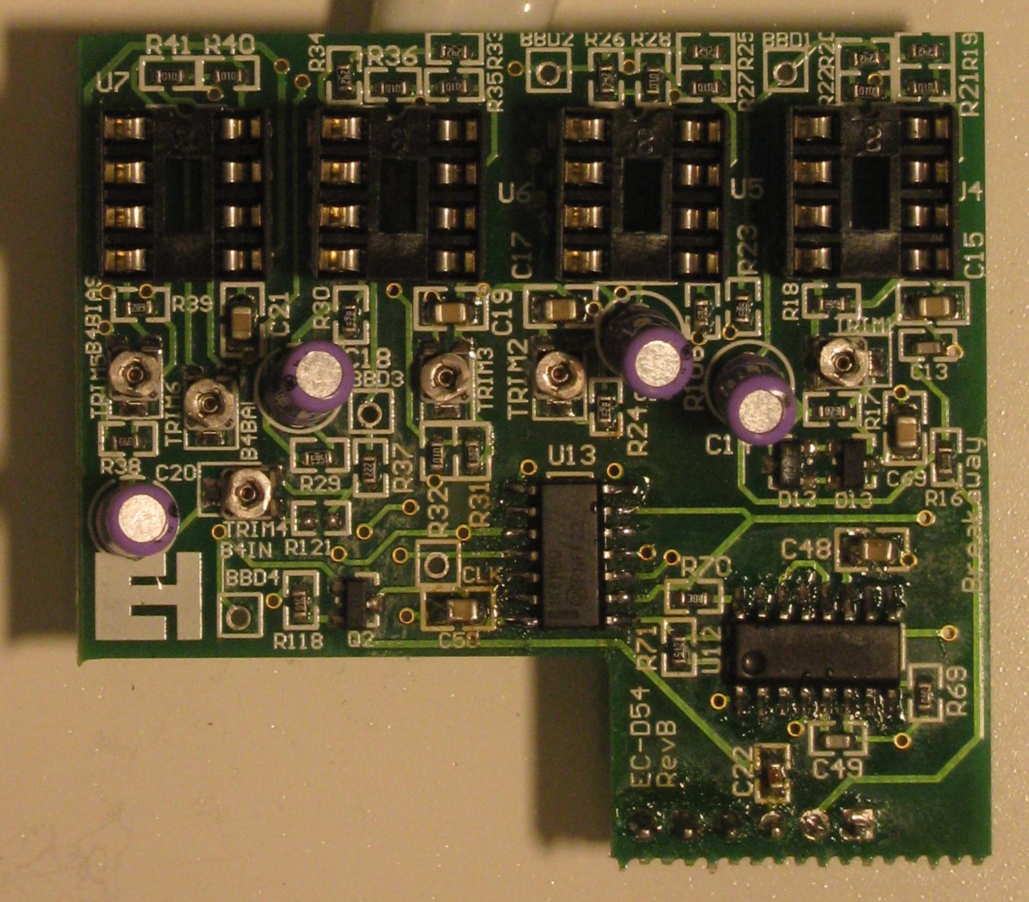
It's a two PCB assembly, all surface mount ICs and passives. The main board appears to handle the input/output buffering, switching, modulation LFO and controls. The smaller daughterboard holds the BBD chips (4x BL3208A), the clock circuit and biasing and balancing trimmers.

Everything is analog, and apart from the BBDs EHX are only using common jellybean parts - SA571 companders, TL074, LM324 & 4558 opamps, LM13700 OTAs. These pedals should be repairable as long the SMD packages can be reworked (they can). The daughterboard is soldered to the main PCB with a 6 pin header strip, and there are some rubber pedal "feet" underneath to support it. I'm not a huge fan of this type of construction, anchoring the small PCB at one edge will allow it to lever and possible damage it. From what I've seen, the Memory Toy uses a similar construction method but the daughterboard is supported at two sides and is socketed instead of soldered. I desoldered the daughterboard to see if there were any backside components (none).
Main board - EC-D54 Rev. B

BBD Board -EC-D54 Rev. B. U13 was removed at this point.


After checking voltages at several ICs I started poking around with the oscilloscope. CMOS logic is used alongside analog ICs so 9V can be used everywhere, there are no voltage regulators onboard.
There is a helpful "CLK" test point on the smaller PCB that showed that I was getting no clock signal to the BBDs. There is a HEF4011 quad NAND-gate in use as an oscillator and an LM13700 configured as either a voltage-controlled resistor or capacitor to vary the frequency of oscillation, controlled by the modulation LFO.

I couldn't see any activity on the NAND chip (U13), so that was suspect. Lifting off the chip showed how it was connected on the PCB. I replaced the 4011 with a new one and the clock signal returned at the CLK test point. The clock frequency varies from about 5 kHz to 100 kHz. For 4 2048 stage BBDs this gives delay times from about ~40 ms to ~800ms, which seems correct. This means that bandwidth is limited to a few kHz at longer delay times,  which gives the characteristic dark sound. LFO is around 0.5 Hz in the slow ("chorus") setting.

After putting it back together it sounds great. I had some pretty bad clock noise at maximum delay time but this went away when I got it back inside the enclosure. Longer repeats are dark, and I don't hear much distortion (though I'm not sure if I would recognize if it was there). Modulation is nice, I find the triangle wave much more useful than the square. It doesn't do the clean repeats with strong attack that digital delays allow, but that's probably not what it's meant to do either.

I don't know why the 4011 failed. I did notice that the specific part used is only rated for ~1mA output current, it's possible that driving the input capacitance of the BBDs at high clock frequencies exceeded this (?) To be safe I used a MC14011 that can supply 8.8mA.

As for scope for mods, a dedicated modulation speed control would be nice. This can be done through the expression pedal jack but as it's only a single resistor in the LFO circuit controlling the rate I may attempt it there. It doesn't really oscillate when feedback is at maximum, so a series resistor with the feedback pot might have be jumpered to get it to break into oscillation.