Thursday, 31 January 2019

Another Electro-Harmonix Freeze

I got another Electro-Harmonix Freeze fairly cheap, it sounded like it had been killed by an incorrect wrong power supply. I took it apart and found that it was a newer revision than I had seen before, the board was EC-D68 Rev C (the last one was Rev B). The main difference I notice was an AK4558 codec instead of PCM3052A.

Freeze Rev C PCB, flash ROM temporarily removed.
Main PCB, LM317 temporarily removed.

There was no sign of life, I found that the series Schottky diode at the 9V input had failed open-circuit and that the LM317 had an internal short between it's input and output pins. The fast/slow/latch mode switch also fell to pieces when the board came out of the enclosure.

I replaced the bad diode with an SS14L (it was the correct size and I already had some at hand) and installed a new LM317. I thought that the LM317 was supplying 3.3V to the DSP and this would fix everything. Instead, the pedal would pass a clean signal but with a clicking sound once or twice per second. I found out that LM317 is actually used as a 1.25V regulator, which is only used for the analog VCC of the DSP56374.

I thought the clicking may be the DSP watchdog timer firing, possibly because it was missing program code, so I removed the flash memory and dumped it. It was a perfect match for the dump I made of the first pedal I repaired, so no problem there.

Measuring power at every IC I found that the 5V rail was high at around 5.9V and the 3.3V supply was sitting at 3.9V. I thought that U5 and U8 (both SOT-89 packages) were also voltage regulators and that maybe they had been damaged as well. I also noticed that U6 is connected to the reset pin of the DSP, and it was resetting the DSP every second or so. My guess is that U6 (also connected to the 3.3V supply) is some kind of voltage supervisor and it is resetting the DSP because of an incorrect 3.9V at VCC.

I found a great picture at freestompboxes (thanks to Steven_M!) showing that on previous version, U5 was 78L05 (5V regulator) and U8 was BA932 (who knows, but from context it has to be a 3.3V regulator).

U5 & U8 on another revision.

The Rev C board in front of me had "BA420" on both chips. Possibly EHX decided to run all 5V parts off of 3.3V, and doubled up on regulators? I don't know.an

To test this out, I decided to remove both chips and apply 5V and 3.3V from  external power supplies.

U5 & U8 removed, external power applied

This set up was a little awkward, but everything work correctly. Current draw looked totally reasonable, 19mA from the 5V supply and 21mA from the 3.3V. No resetting, no clicking, and the pedal could freeze audio in all 3 modes.

Current draw on 5V and 3.3V supplies.

I ordered L78L05ABUTR and MCP1804T-3302I/MB as replacement 5V and 3.3V SOT-89 regulators. I also used 2MD3T2B2M2RE as a replacement switch. This replacement is not threaded for a nut, but recent version of the Freeze don't look like they are threaded either. Pedal works like new.


Ibanez DDL10 Delay II

This is another early digital delay pedal, I am guessing it was built in 1986 from some of the IC date codes. I don't know if the 10 series included the first Ibanez/Maxon digital delay. Obviously this is the "Delay II", but the DDL Delay I and Delay III were also released in the same series of pedals,  each with different delay times. The max delay time of 900ms of the Delay II put it in a similar league to the Boss DD-2.


Inside, there is a two PCB construction with a hard-wired ribbon cable. The top board has unpopulated parts, I would guess that a DML10 (modulated delay) could be built on this same board by populating an opamp LFO and adding the two extra pots.

DDL10 internals

The bottom PCB has two 4164 DRAMs, an NE571 compoundor, LM311 comparator (most likely used as part of an ADC as in the DD-2 and PDS delays) and a bunch of opamps. The SIL (single in-line) package chips are M5218L low-noise preamplifiers, used in lots of Japanese pedals. There are only 2 4164 64kb DRAMs, the DD-2 has 3. Either the DD-3 has higher sampling rates, or the Ibanez uses 8-bit samples instead of 12-bit. This is still more than the single 64k seen in Digitech PDS 1 second delays.

Main PCB, component side

The back side of the lower board just has a main controller MC4101F IC. I can't find any info on this, it's almost certainly a custom controller for digital delays (like the Boss/Roland RDD63H101).

Main PCB, back-side.

This unit looked mostly dead, it passed no effected signal and LED didn't respond to the footswitch. I thought the back of the larger board looked a bit crusty so I clean it with 99% IPA, afterwards I saw the LED blink with the footswitch. Still no signal.

I couldn't find any schematics for this model online, but someone has scanned and uploaded an Ibanez factory schematic for the DFL10 flanger from the same series, which uses the same controller IC. There is a full pinout.

DFL10 schematic page 1.
DFL10 schematic page 2.

From the schematic, the clock signal for the controller looked like it was coming from a VCO to pin 26 ("2F"). I probed my board and found that I did have a clock signal, it could be varied by turning the Delay knob, and I also had what looked like communication between the controller and the RAM chips.

At this point I got really lucky. There was a 100uF electrolytic capacitor near the LM311 comparator that was a little discoloured. While taking measurements I noticed it was getting warm. I pulled it from the circuit, and the pedal started passing a delayed signal. This cap is connected from 5V to ground right next to the comparator input, if the cap was leaky then it would effectively mute the comparator. Everything worked without this capacitor, I replaced it anyway with a new low profile 100uF for peace of mind.

Faulty capacitor pulled.
The LED turned out to be a bad solder joint - it would light sometimes if it was held in a certain position. Reflowing the joints fixed it.

Way Huge Aqua Puss MK II

I don't think I've ever looked at anything by Way Huge before. This is a modern version of the Aqua-Puss, and Jim Dunlop acquired Way Huge in 2006, so I expect it to be similar to the current Dunlop and MXR stuff.

This one would light it's LED when switched on but wouldn't pass a signal.


The insides are really nice, and very easy to disassemble. There are three PCBs - one just breaking out the switch contacts, one SMD board for input/output and switching and one through-hole board with the effect guts. They probably re-use the two smaller PCBs for all of the pedals in this size of enclosure.

Interior

The upper board has a CD4013 dual flip-flop, a CD4093B quad NAND gate and a relay to handle the bypass. The manual says the pedal has "AC protection", I don't know if this is just a series Shottky diode or something more sophisticated. There are some opamps and what looks like a IRF7606 Mosfet in a micro-8 package, that could be doing some power switching in case of reverse polarity or an AC supply connected. Relay is a EA2-5SNJ, similar to what's in a DL4.

I/O & switching board component side

Jack side

The delay board a V3205 BBD and BL3102 clock generator, SA571 compoundor and LF353 opamp for input and output buffering. Freestompboxes.org has the full schematic, it's not too complex a delay and similar to a DM-2/DM-3.

Pinout of the 8-pin connector is as follows (taking the pin with square PCB footprint as pin 1)
  1. 9V
  2. Ground
  3. LED
  4. Bypass switch
  5. Input signal
  6. Output signal
  7. Relay coil
  8. Relay coil 
The relay coil contacts are probably only broken out so the small PCB can be connected to a test jig, the main board doesn't route them anywhere.

Delay board component side

Delay board back side


I couldn't tell if the relay was actually switching, as it was hard to hear it click over the sound of the footswitch. When I disconnected the foot switch board and triggered the switch with some wire I could hear the relay clicking, so the switching logic was probably good.

After hooking up a test signal and oscilloscope I could see that the input signal was reaching the first opamp stage but there was nothing at the output pin. I desoldered the LF353 and replaced it with a socket and a TL072 for now.

Removed LF353

Now I had a clean signal in bypassed mode, but no delay. No switching waveforms on the BBD on the oscilloscope. No power at either the clock generator or BBD either. The schematic shows an NPN transistor/diode voltage regulator for these chips, I found that the 2N3904 transistor was blown to shit! After replacing with a new 2N3904 it regulator to around 7.4 volts. I'm not totally sure why this is needed as the BL3102 & V3205 should be happy to run on 9V, this may be a holdover from using older BBD chips. (Update: it turns out that there are multiple V3205 datasheets online, with conflicting information. According to Coolaudio, the max Vdd for a V3205SD is 8V).

Epoxy case blown off voltage regulator pass transistor. I don't know how I missed this.

I could now see clock signal at the BBD which varied with the delay knob as expected, but still no delay. I could see an input signal at pin 11 of the SA571 but nothing at the output on pin 10. I borrowed an SA570 from PDS delay pedal and this brought back the delay effect. Sounds great but not too different from other analog delays I have.

So: dead 2N3904 regulator, dead LF353 and dead SA571. I'm guessing this was fed too high a voltage from the wrong power supply. It's running happily 24 hours later with a new SA571 so this will probably go up for sale on Reverb pretty soon.

Friday, 7 December 2018

Silvertone Bass 35


This is a cool little solid state bass amp, I'm guessing dating to the 60s. No idea if Silvertone manufactured this, or if it was a rebrand, as there is very little information about this model online.

Solid State Bass 35

No output signal. Only 5 transistors, so surely this would be easy? Instead of getting through this quickly I had it for several months, only looking at it when I had a few minutes to spare. If I had more space to work with this could have been much faster and easier. This has been a trend with physically large gear, I should really think about learning a lesson and getting a wide bench and keep it clean somehow.

Single sided phenolic PCB

Full of cracks and mild corrosion

This amp has been worked on in the past, and has some of the electrolytics replaced. It was also dropped on it's faceplate at some point in the past, and the phenolic PCB has cracked. The ground pour is broken in a few places and it has been bridged with solder.


Original output transistors.

Most of the transistors appear to be branded with house-markings, as I can't find any references to their part numbers. I initially though output transistors were bad. They are marked "761" and "CG121", no info on these. One seemed to have a very low Vbe when measured with a DMM diode mode, which looked like a shorted junction. The TO-3 pinout is fairly standard for transistors, so I was assuming all cases were collectors. Collectors voltages were +35V and 0V, so I made guesses as to which output transistors were NPN and PNP types and then replaced with new 2N3055 and MJ2955 in TO-3 packages, new mica washers and new thermal grease.

Dead bass control/driver transistor

After tracing the signal through the amp with a scope I found that nothing was getting to the output transistor bases. Nothing was passing the third transistor that drives the output transistors and implements the bass control. It was marked "5981 274 S6721", no idea. I desoldered this part and found that it was dead, completely shorted leads. I replaced this with a BD139. Based on a guess of the polarity of the original and the size of that package I thought this should handle the current requirements. With the BD139 I got some life, there was an output signal sometimes. Turning power on and off would sometimes get it working, sometimes it would stop. I found that there was a high-frequency oscillation at the output stage, if it drifted in and out of oscillation then things would work. Capacitors from collectors to base pins fixed this, values were just picked experimentally.

It still didn't sound right. There was an odd overtone riding on top of the signal that couldn't really be dialed out, though it sounded better at higher volumes. Another parasitic oscillation? Bias issue?

Around this time I bought a Peak Atlas DCA 55 Semiconductor tester. This is a very useful tool for testing transistors and diodes, and will also attempt to identify parts based on I/V characteristics. I still had the original TO3 power transistors, so I tried them out. One read a Vbe of 0.19V but was identified as PNP germanium, and working. I had assumed Vbe this low was a problem. After putting the old transistors back into the amp with new grease it sounded great, not very clean but not totally distorted either. The replacement silicon part wasn't biased correctly, the odd sound was probably some crossover distortion.


There is a diode from the base of CG121 which is probably used for biasing, I would guess that this is also germanium and modifying the amp to use new silicon transistors would involve replacing this as well.

The replacement BD139 runs quite warm, but not so much that I would worry about heatsinking it yet.

Here are measurements of the originals, they are surprisingly mismatched. This may not be a push-pull design at all.

7671
NPN silicon
hfe 108 @ Ic 2.5 ma
Vbe 0.643V

cg121
PNP germanium
hfe 59 @ Ic 2.5 mA
Vbe 0.190V
Ib 4.781 mA


Hopefully this is good for another 40 years.

Thursday, 22 November 2018

Red Panda Particle

It's been a while. I have been doing repair jobs and not posting them, so I will try to clear the backlog.

I bought a non-working Red Panda Particle granular delay for a decent price. This is fairly well documented as a Spin FV-1 design, but the granular delay programs and pitch-shifting & randomised modes really drew my interest.


The insides are fairly simple - the FV-1, a 24LC32a serial EEPROM, a 74HC148 priority encoder (to decode the rotary switch and select which program to run) and a quad OPA4134 opamp. The "chop", "delay/pitch" and "param" pots are read by the FV-1, the blend and feedback controls appear to be done in the analog domain. This looks more or less like a reference FV-1 design, all the magic is in the program code.

The PCB layout is nice, pots and jacks are board-mounted and the DC jack is on a connector so the entire board can be removed or tested before installing in an enclosure. They use a PCB mounted spring to ground the enclosure, like the modern EHX designs, but this one seems to be contacting an oversprayed section.

Interior layout.

This pedal passed no signal in effected mode. I probed the OPA4134 and the first opamp that drives the mix control was stuck at near ~8V DC. After replacing the chip everything worked.

IC10 removed.


This is a really cool design, in that it's very different to nearly every delay I've used before. It is quite difficult to predict how the different modes will sound, and I think this would need some significant playtime to learn. Unfortunately this one came along at a time when I didn't have a lot of free time or desire to keep amassing pedals, so I have sold it on.

I did dump the EEPROM. Looking at it briefly with the excellent online FV-1 decompiler, each program looks to have disassembled correctly and makes some sense. I'm reluctant to share this, as this is really the only unique part of the pedal, and AFAIK it hasn't been cloned. If you have a genuine repair need (pedal with dead ROM) then get in touch, maybe I'll help. I may also revisit this and get it running on a different FV-1 board at some point in the future.

Thursday, 1 March 2018

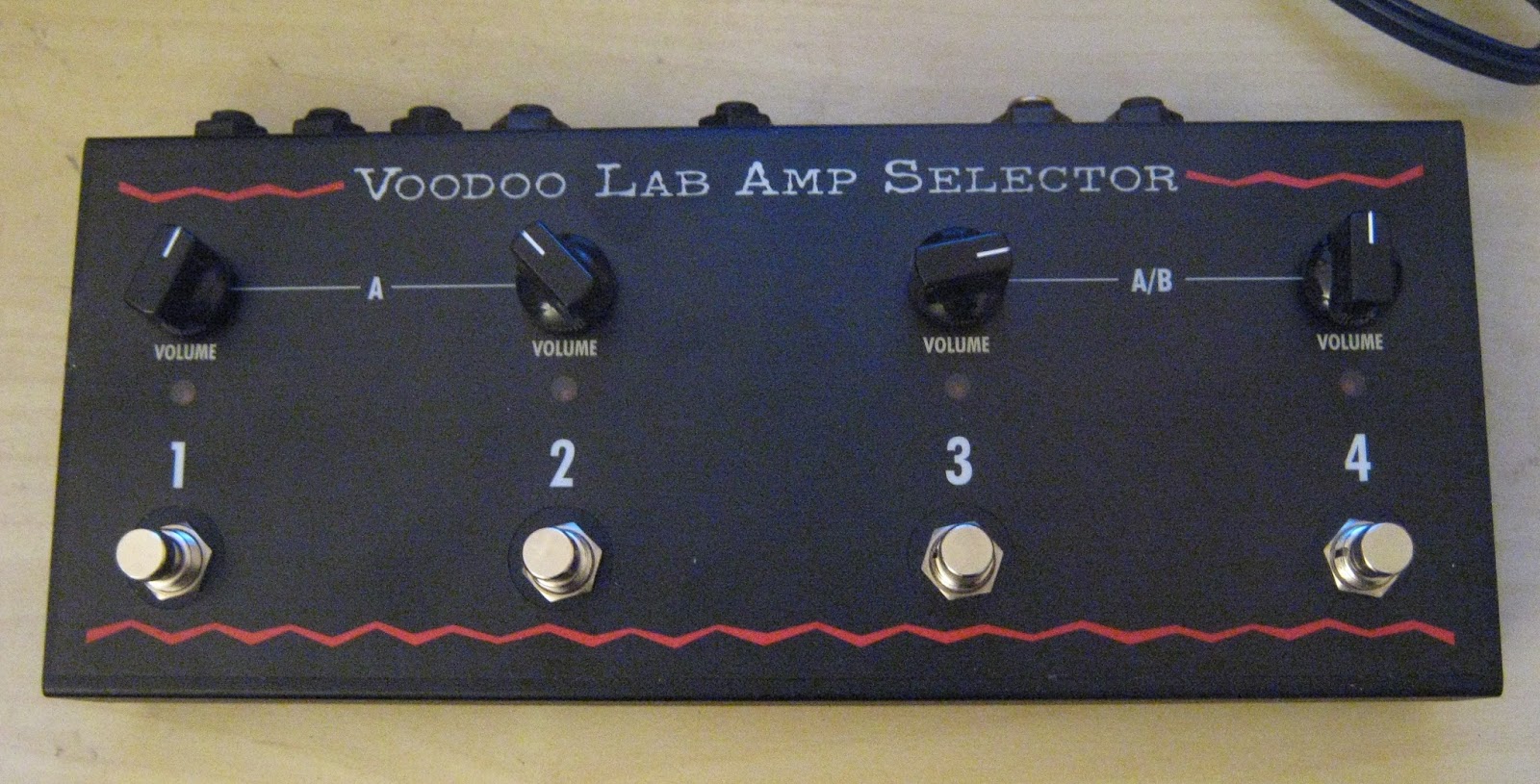
Voodoo Labs Amp Selector

 This is a 2 input, 4 output amp selector and A/B switch. One guitar can drive 4 isolated outputs, all with their own volume controls and ground lifts. There is some preset save/recall functionality, so I am expecting a microcontroller in here somewhere. This is exactly the sort of thing I would have loved to play with when I was renting a practice room and had access to lots of amps, but it will probably just be sold on nowadays.


Main PCB
No surprises on the insides - there is an P87LPC764 MCU reading switches and turning JFET switches on and off. A MAX1044 provides a -9V supply. The transformers are 6 pin devices with any labels or markings removed. There is one OPA2134 dual opamp, and a 24C01 serial EEPROM for presets.

Hacked in parts at the power input.
The back of the PCB has some factory bodges/mods at the power input - there is a series resistor and a capacitor added to the MAX1044 input.

The digital side seemed to work, everything lit up and it did switch signals, but there was lots of bleed between outputs and the volume was quite weak.

I know from experience that a MAX1044 will only tolerate ~10V input before dying, so I looked there first. The inverted voltage was measuring less than -1V. I desoldered the MAX1044 and replaced it - no change. There is a zener diode at the input pin which should limit the input voltage, I lifted this part out and now I had -8V and a working pedal.

Replaced MAX1044 (pictured here sitting crooked in a socket) and lifted diode D10
This diode was a 1n5239b (9.1V 0.5W zener) so I replaced it with a 1W part I had at hand. Now the negative voltage was pulled low again! It turned out that the cap across the zener that was added to the packside was leaking. It still measured 2.2uF but had ESR >5 ohm - this looks like a dipped tantulum part. I replaced with a similar electrolytic. It's not even technically needed, the cap is just stabilising the 9.1V zener clamp when it's conducting.

TC Electronics Nova Drive NDR-1

Programmable overdrive & distortion from TC Electronics. All overdrive/distortion parameters are controlled digitally, so presets can be saved and recalled, the order of the two circuits can be changed, they can be run in series or in parallel. All of this can be triggered by MIDI.


 TC did a Nova series of pedals and multi-effects units, but I don't think they were all built around a common digital design (like the Line 6 4x4 series). TC stuff is interesting as they have a history of high quality and targeting high-end markets and they tend to use fairly modern designs and parts. Unfortunately they don't seem to release much information or contract out any repair services, so I have not come across any modern TC Electronics schematics, either official or leaked.
TC were sold to Behringer in 2015 and their latest range of pedals look to be more standard stuff, a bit watered-down compared to the Nova series. I'll reserve judgement until I see one.
This series used a 12V power supply for some reason (why not 9V, like everything else?)
This Nova Drive started up but only passed a signal in bypass mode. The LED display and indicators did react to the knobs and to button presses, which at least meant that the digital section is working and the problem was likely in the analog end.

Top PCB (digital)
The build quality is really nice, they use a folded and tapped sheet metal chassis instead of cast box. There are two PCBs inside, the first is a "mezzanine" board with the encoders, buttons and displays. There is an Atmel ATmega168 and some '595 and '165 shift registers for digital IO. I'm pretty sure the ATmega is reading out pots and buttons and controlling something on another PCB to vary the effect parameters, as well as driving the LED displays and responding to MIDI commands. I would guess that this top PCB is probably very similar across all the Nova pedals. I am assuming the ATmega has some code-protection so I haven't tried desoldering and dumping it.

Lower PCB (analog)

The bottom PCB fills the whole enclosure - it has a bunch of opamps (presumably the analog overdrive and distortion circuits), DG441D quad analog switch ICs, switching power supplies, the MIDI optoisolator, a relay and a Cirrus CS3308. The CS3308 is a cool part, it's an 8-channel digitally programmable volume control. Presumably each channel is mapped to one encoder (4 knobs for overdrive and 4 for distortion) and the ATmega sets the levels over SPI or I2C. TC have used the +-5V version with 123 dB of dynamic range, which is kind of ludicrous for a distortion pedal.

Lower PCB, backside

U3 generates -12V from 12V input

All parts on this side are glued in placed before soldering

The bottom PCB is very parts-dense, but helpfully there are test points for all supply voltages. I found that -12V was reading very low and so all of the negative supplies that are derived from -12V were also missing. -12V appeared to come from a switching supply controlled by a CS51411 on the underside of the PCB, the circuit looks liked a close match to the inverting converter in the datasheet (Fig 25). The inductor was getting burning hot, so the switching IC was a pretty likely culprit. TC used a double sided load for this PCB, and parts on the underside are wave-soldered instead of reflowed, which means they are all held in place with a dot of red epoxy. Desoldering the IC took a lot more heat and force than I'm used to but it did eventually lift off. It still didn't work with a new chip, solid 12V DC across the inductor with no switching happening, which explains the heating. The SYNC pin did have a ~340 kHz square wave - I don't know if this was also present on the original chip. The huge number of test points on the back of this larger PCB suggests TC use some kind of bed-of-nails jig for testing during manufacturing.

Around this time I held my hand over the board when powered up and found another hot spot. One of the two DG441D switch ICs was also running hot, so I desoldered it. This part does run off +12V and -12V rails, so it may have killed the -12V supply when it failed.

There is another switching power supply using a L5970D controller - this one is generating 3.3V for the digital parts and was working correctly.

As I knew there may have been a short from -12V to ground or some other supply, I wanted to see if I could completely isolate the CS51411 from the -12V supply and use an external power supply to provide -12V. I removed the output capacitor and the inductor. Using an bench supply wired to the board and providing -12V, the pedal worked. Surprisingly, it pulled over 100 mA which seemed very high for some opamps and switch ICs so there may have been some other damaged part on that -12V rail.

The series/parallel switching did not work, only series mode passed a wet signal. This confirms the DG441Ds are routing the signals into series or parallel combinations, one of them was still missing. A new IC here restored all modes.

The CS51411's inductor measured 33uH out of circuit which seemed correct. I decided to try swapping it with this part, which fixed all the power supply issues. I am guessing that the old inductor got so hot that it reached it's curie temperature and it's magnetic properties changed (??) The new part runs cool. Looking again at the CS3308 datasheet shows it pulls 36 - 50 mA on both positive and negative analog supplies (!), which explains the high power consumption seen earlier, and why the pedal originally shipped with a 12V supply rated for 400 mA. This chip does run noticeably warm, but the power consumption matches the datasheet figures. I can only guess that power consumption is targeted  high to help lower noise and increase dynamic range. For a distortion pedal a low-power version with poorer specs would probably be a much better fit. The pedal will actually work with 9V input, and will generate a -9V supply instead, but will need a beefier supply than is usually seen on pedalboards.

All good again.
I broke the ribbon cable connecting the two boards when I was working on this. I just replaced it with individual wires - I would really like a tool that strips ribbon cable so I could just buy a small reel, if anyone knows of one please let me know.